Replacing the TDK 78P7200/2241
时间:2009-04-20 | 栏目:通信网络 | 点击:次
Abstract: This application note provides the information required to use the DS3150 line interface unit (LIU) in place of the TDK 78P7200, TDK 78P200L, and TDK 78P2241. The DS3150 LIU performs all the functions necessary for interfacing at the physical layer to T3, E3, and STS-1 lines.
Introduction
The DS3150 is a full-featured line interface unit (LIU) that performs all of the functions necessary for interfacing at the physical layer to T3, E3, and STS-1 lines. The DS3150 is pin compatible with the TDK 78P2241, 78P2241B, and 78P7200L devices and an easy replacement for the 78P7200. The purpose of this application note is to describe how to replace the TDK devices with the DS3150 in existing designs. This application note should be read in conjunction with the DS3150 data sheet and the relevant TDK data sheet(s).Replacing the 78P2241, 78P2241B, and 78P7200L with the DS3150
Although for new designs the DS3150 data sheet recommends somewhat different external components than those used with these TDK devices, the DS3150 can be dropped into existing 3.3V designs with no changes to the board artwork and no component changes, if the wiring recommendations in the TDK data sheets were followed. Since the DS3150 is a 3.3V-only device, it cannot replace the 78P2241 devices in 5V applications unless it is provided with a 3.3V supply. TDK's recommended wire-up for the 78P2241 devices configures the DS3150, as shown in Table 1. TDK's recommended wire-up for the 78P7200L configures the DS3150, as shown in Table 2.Replacing the 78P7200 with the DS3150 in Existing Designs
To replace the 78P7200 in an existing design, the following changes are required. See Figure 1 for component locations.- Provide a 3.3V power supply to the DS3150 rather than the 78P7200's 5V supply.
- Replace the CPD capacitor with a 0Ω resistor.
- For E3 applications RTT should be 301Ω.
- For best impedance matching, change RTR to 330Ω.
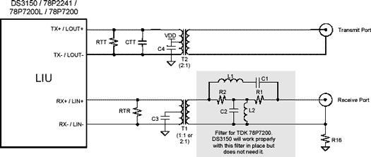
Figure 1. Line interface external components.
The CPD pin on the TDK 78P7200 is used to place a decoupling capacitor between the peak detector node and VCC. On the DS3150, the CPD pin function is not required and the pin is reassigned to be the loopback control input active-low LBKS. Replacing the CPD capacitor with a 0Ω resistor results in active-low LBKS being pulled up to VCC, disabling loopbacks in the DS3150. If the DS3150 is used in an existing 78P7200 design, TDK's recommended wire-up of the 78P7200 plus the required changes above configure the DS3150, as shown in Table 3.
Table 1. Pin-by-Pin Look at the DS3150 in a 78P2241 Application
| PLCC Pin # | TQFP Pin # | 78P2241 Pin | DS3150 Pin | 78P2241 Recommended Wiring: Effect on DS3150 Operation |
| 1, 3 | 42, 44 | LIN+, LIN- | RX+, RX- | 75Ω termination resistor and 1:1 transformer gives actual line termination of approximately 73Ω. Receiver works fine. |
| 2 | 43 | GND | EFE | EFE=0 disables DS3150 enhanced features. |
| 4 | 46 | GND | TDS0 | TDS0=0 has no effect. EFE pin tied low causes DS3150 to ignore this pin. |
| 5 | 2 | RFO | TDS1 / OFSEL | Resistor RFO to ground has no effect. MCLK pin internally pulled up causes DS3150 to ignore this pin and use TCLK as master clock. |
| n/a | 8 | GND | DM* | Open-drain DM* output tied to ground is no problem. |
| 9, 11 | 9, 11 | LOUT+, LOUT- | TX+, TX- | 301Ω termination resistor and 2:1 transformer gives actual line termination of approximately 69Ω. Transmitter works fine. |
| 10 | 10 | ICKP | ICE | DS3150 pin function matches 78P2241 pin function. |
| 12 | 13 | LBO | DS3150 pin function matches 78P2241 pin function. | |
| 13 | 15 | E3* | TESS | DS3150 pin function matches 78P2241 pin function. |
| 14 | 16 | TPOS / TNRZ | DS3150 pin function matches 78P2241 pin function. | |
| 15 | 17 | TNEG | DS3150 pin function matches 78P2241 pin function. | |
| 16 | 18 | TCLK | DS3150 pin function matches 78P2241 pin function. | |
| 18 | 22 | TXEN | TTS* | DS3150 pin function matches 78P2241 pin function. |
| 19 | 26 | LF1 | MCLK | Capacitor to ground is no problem. Internal pull-up to VDD pulls MCLK high, causing DS3150 to use TCLK as its master clock. |
| 20 | 27 | ENDEC* | ZCSE* | DS3150 pin function matches 78P2241 pin function. |
| 21 | 28 | MON | RMON | DS3150 pin function matches 78P2241 pin function. |
| n/a | 29 | GND | PRBS | PRBS output tied to ground is no problem. EFE pin tied low causes DS3150 to tri-state this pin. |
| 23 | 33 | RCLK | DS3150 pin function matches 78P2241 pin function. | |
| 24 | 34 | RNEG / RLCV | DS3150 pin function matches 78P2241 pin function. (Only 78P2241B has LCV function when ENDEC*=0) | |
| 25 | 35 | RPOS / RNRZ | DS3150 pin function matches 78P2241 pin function. | |
| 27 | 39 | LOS* | DS3150 pin function matches 78P2241 pin function. | |
| 28 | 40 | LPBK* | LBKS* | DS3150 pin function matches 78P2241 pin function. |
| 6-8, 17, 22, 26 |
1, 3-7, 12, 14, 19-21, 23-25, 30-32, 36-38, 41, 45, 47, 48 |
VSS, VDD | VDD must be 3.3V. | |
Table 2. Pin-by-Pin Look at the DS3150 in a 78P7200L Application
| PLCC Pin # | TQFP Pin # | 7200L Pin | DS3150 Pin | 78P7200L Recommended Wiring Plus Required Change: Effect on DS3150 Operation |
| 1, 3 | 42, 44 | LIN+, LIN- | RX+, RX- | 75Ω termination resistor and 1:1 transformer gives actual line termination of approximately 73Ω. Receiver works fine. |
| 2 | 43 | GND | EFE | EFE=0 disables DS3150 enhanced features. |
| 4 | 46 | GND | TDS0 | TDS0=0 has no effect. EFE pin tied low causes DS3150 to ignore this pin. |
| 5 | 2 | RFO | TDS1 / OFSEL | Resistor RFO to ground has no effect. MCLK pin internally pulled up causes DS3150 to ignore this pin and use TCLK as master clock. |
| n/a | 8 | GND | DM* | Open-drain DM* output tied to ground is no problem. |
| 9, 11 | 9, 11 | LOUT+, LOUT- | TX+, TX- | 301Ω termination resistor and 2:1 transformer gives actual line termination of approximately 69Ω. Transmitter works fine. |
| 10 | 10 | ICKP | ICE | DS3150 pin function matches 78P7200L pin function. |
| 12 | 13 | LBO | DS3150 pin function matches 78P7200L pin function. | |
| 13 | 15 | E3* | TESS | DS3150 pin function matches 78P7200L pin function. |
| 14 | 16 | TPOS | TPOS/TNRZ | DS3150 pin function matches 78P7200L pin function when ZCSE*=1. |
| 15 | 17 | TNEG | DS3150 pin function matches 78P7200L pin function when ZCSE*=1. | |
| 16 | 18 | TCLK | DS3150 pin function matches 78P7200L pin function. | |
| 18 | 22 | TXEN | TTS* | DS3150 pin function matches 78P7200L pin function. |
| 19 | 26 | LF1 | MCLK | Capacitor to ground is no problem. Internal pull-up to VDD pulls MCLK high, causing DS3150 to use TCLK as its master clock. |
| 20 | 27 | N/C | ZCSE* | Internal pull-up disables DS3150 B3ZS/HDB3 encoder/decoder and puts DS3150 into bipolar interface mode, which matches 78P7200L behavior. |
| 21 | 28 | N/C | RMON | RMON floating is a valid state: 20dB pre-amp disabled, jitter attenuator enabled in the receiver path. |
| n/a | 29 | GND | PRBS | PRBS output tied to ground is no problem. EFE pin tied low causes DS3150 to tri-state this pin. |
| 23 | 33 | RCLK | DS3150 pin function matches 78P7200L pin function. | |
| 24 | 34 | RNEG | RNEG/RLCV | DS3150 pin function matches 78P7200L pin function when ZCSE*=1. |
| 25 | 35 | RPOS | RPOS/RNRZ | DS3150 pin function matches 78P7200L pin function when ZCSE*=1. |
| 27 | 39 | LOS* | DS3150 pin function matches 78P7200L pin function. | |
| 28 | 40 | LPBK* | LBKS* | DS3150 pin function matches 78P7200L pin function. |
| 6-8, 17, 22, 26 |
1, 3-7, 12, 14, 19-21, 23-25, 30-32, 36-38, 41, 45, 47, 48 |
VSS, VDD | VDD must be 3.3V. | |
Table 3. Pin-by-Pin Look at the DS3150 in a 78P7200 Application
| PLCC Pin # | 78P7200 Pin | DS3150 Pin | 78P7200 Recommended Wiring Plus Required Changes: Effect on DS3150 Operation |
| 1, 3 | LIN+, LIN- | RX+, RX- | 422Ω termination resistor changed to 330Ω and 1:2 transformer gives actual line termination of approximately 75Ω. Receiver works fine. |
| 2 | NCR | EFE | EFE=0 disables DS3150 enhanced features. |
| 4 | NCR | TDS0 | TDS0=0 has no effect. EFE pin tied low causes DS3150 to ignore this pin. |
| 5 | RFO | TDS1 / OFSEL | Resistor RFO to ground has no effect. MCLK pin internally pulled up causes DS3150 to ignore this pin and use TCLK as master clock. |
| 9, 11 | LOUT+, LOUT- | TX+, TX- | 301Ω termination resistor and 2:1 transformer: actual line termination is approximately 69Ω. Termination resistor must be the same for E3 mode. Transmitter works fine. (Changing resistor to 330Ω results in actual line termination of approximately 75Ω.) |
| 10 | NCT | ICE | Tied to ground: DS3150 matches 78P7200 behavior. |
| 12 | LBO | DS3150 pin function matches 78P7200 pin function. | |
| 13 | OPT1* | TESS | DS3150 pin function matches 78P7200 pin function. Although the preferred wiring of TESS for STS-1 is to leave it floating, the DS3150 will handle STS-1 correctly with TESS pulled high. |
| 14 | TPOS | TPOS/TNRZ | DS3150 pin function matches 78P7200 pin function when ZCSE*=1. |
| 15 | TNEG | DS3150 pin function matches 78P7200 pin function when ZCSE*=1. | |
| 16 | TCLK | DS3150 pin function matches 78P7200 pin function. | |
| 18 | OPT2* | TTS* | DS3150 pin function matches 78P7200 pin function. |
| 19 | LF1 | MCLK | Resistor to LF2/ZCSE*, capacitor to ground is no problem. With resistor to LF2/ZCSE* and resistor from LF2/ZCSE* to VCC, MCLK is pulled up, causing DS3150 to use TCLK as its master clock. |
| 20 | LF2 | ZCSE* | Resistor to VCC disables DS3150 B3ZS/ HDB3 encoder/decoder and puts DS3150 into bipolar interface mode, which matches 78P7200 behavior. |
| 21 | NCD | RMON | RMON=0 disables DS3150 20dB pre-amp and Rx Jitter Attenuator. |
| 23 | RCLK | DS3150 pin function matches 78P7200 pin function. | |
| 24 | RNEG | RNEG / RLCV | DS3150 pin function matches 78P7200 pin function when ZCSE*=1. |
| 25 | RPOS | RPOS / RNRZ | DS3150 pin function matches 78P7200 pin function when ZCSE*=1. |
| 27 | LOWSIG* | LOS* | DS3150 pin function matches 78P7200 pin function. |
| 28 | CPD | LBKS* | Capacitor to VCC must be changed to 0Ω resistor to disable DS3150 loopbacks. |
| 6-8, 17, 22, 26 |
VSS, VDD | VDD supply must be changed from 5V to 3.3V. | |